Effect of Mechanical Stress on AlGaN/GaN High Electron Mobility Transistor (HEMT) Device Characteristics and Reliability
AlGaN/GaN HEMTs are regarded as promising candidate for RF and high power electronics applications due to unique material properties of GaN, such as, wide band gap, high breakdown field, high carrier mobility, and large saturation velocity. Other advantageous characteristics, such as, piezoelectricity and spontaneous polarization within AlGaN and GaN layers result in high 2D electron gas densities. However the wide deployment of the AlGaN/GaN HEMT technology is currently hindered due to its limited electrical reliability. Achieving high-level of reliability concurrently with high power operation remains an important challenge for this technology. Improvements in the reliability of these devices require a thorough understanding of the failure mechanisms that degrade the device performance.
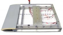
Studies show that AlGaN/GaN HEMTs degrade significantly under typical device operation. Degradation in these devices has been hypothesized to occur due to charge trapping, hot electron effects, and crystallographic defect formation due to inverse-piezoelectric effect. GaN HEMTs have high internal stresses resulting from lattice mismatch between GaN and AlGaN layers and generated during device operation due to inverse piezoelectric effect. Mechanical stress impacts the device performance by affecting the carrier mobility, polarization, band-gap, trap energy levels and trap generation and hence influences the reliability of these devices. The goal of this project is to investigate the effect of stress, bias and temperature on device characteristics and understand the fundamental physics governing the device operation; and hence the failure mechanisms that degrade the device performance. Four-point mechanical wafer bending is used to study the effect of stress on AlGaN/GaN HEMT channel resistance and gate current to provide insight on the role of stress in device reliability.


