Nano Technologies

Ultra-High Energy Nanocomposite Capacitors

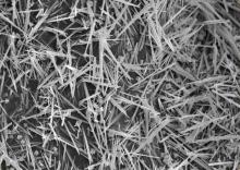
High energy density capacitors are critically important in advanced electronic devices and electric power systems that require bursts of large energy such as pace makers, defibulators, rail guns, electric vehicles and electromagnetic armor.  Our work is studying the use of nanocomposites to create ultra high energy density capacitors with particular focus on the role the morphology and orientation of the filler plays on the energy density.  Our current results have produced nanocomposites with energy density exceeding 10 J/cc, which is more than twice as large as high performance commercial materials.  Efforts to create further gains are focused on the synthesis of new high dielectric ceramic nanowires, approaches for the functionalization of the fillers to achieve improve compatibility with the polymer matrix materials and fabrication approaches to create the highest energy density capacitors available.

Spatially controlled electrospun solid gradient nanofibers for guided spiral ganglion neuron culture

The direction of cell growth is associated with chemical, structural and/or mechanical properties of the substrate. Structurally, electrospun nanofibers provide a suitable environment for cell attachment and proliferation due to their similar physical dimension to that of the extracellular matrix. Furthermore, by modulating the topographical features of nanofibers, which include fiber diameter and orientation, cell growth and its related functions can be modified. Here, we demonstrate a solid gradient scaffold for directional growth of spiral ganglion neurons (SGNs). Spatial nanofiber alignment is controlled using a custom directional electrospinning setup. The electric field to spatially control the confinement of nanofibers was simulated with COMSOL Multiphysics simulation tool and experimentally verified. To promote neurite outgrowth and impart directionality to SGN cells, a spatial gradient of neurotrophin (NT) is introduced. By sequentially electrospinning solutions of increasing concentrations of NT in the biodegradable polymer and collecting sections of these aligned fibers along a uniaxial direction, we achieved uniform sectional nanofibers of increasing gradient concentrations. Initial tests with SGNs show improved cell adhesion and decreased morbidity to microfabricated PLGA scaffolds. Our solid gradient nanofiber membrane is versatile, obviates the need for the complex microfluidic mixer system to generate an NT gradient, is potentially implantable, and can be used in other nerve regeneration studies in peripheral nerve system and central nerve system.

Fabrication of Nanoporous membrane and its non-lithographic patterning using Electrospinning and Stamp-thru-Mold (ESTM)

The Electrospinning and Stamp-thru-mold (ESTM) technique, an integrated fabrication process which incorporates the versatility of the electrospinning process for nanofiber fabrication with
the non-lithographic patterning ability of the stamp-thru-mold process is introduced. In-situ multilayer stacking of orthogonally aligned nanofibers, ultimately resulting in a nanoporous membrane, has been demonstrated using orthogonally placed collector electrode pairs and an alternating bias scheme. The pore size of the nanoporousmembrane can be controlled by the number of layers and the deposition time of each layer. Non-lithographic patterning of the fabricated nanoporousmembrane is then performed by mechanical shearing using a pair of pre-fabricated micromolds. This patterning process is contamination free compared to other photo lithographical patterning approaches. The ability to pattern on different substrates has been tested with and without oxygen plasma surface treatment. In vitro tests of ESTM poly-lactic-coglycolic acid (PLGA) nanofibers verify the biocompatibility of this process. Simulation by the COMSOL Multiphysics tool has been conducted for the analysis of electrospun nanofiber alignment.

Effect of Mechanical Stress on AlGaN/GaN High Electron Mobility Transistor (HEMT) Device Characteristics and Reliability


AlGaN/GaN HEMTs are regarded as promising candidate for RF and high power electronics applications due to unique material properties of GaN, such as, wide band gap, high breakdown field, high carrier mobility, and large saturation velocity. Other advantageous characteristics, such as, piezoelectricity and spontaneous polarization within AlGaN and GaN layers result in high 2D electron gas densities. However the wide deployment of the AlGaN/GaN HEMT technology is currently hindered due to its limited electrical reliability. Achieving high-level of reliability concurrently with high power operation remains an important challenge for this technology. Improvements in the reliability of these devices require a thorough understanding of the failure mechanisms that degrade the device performance.

Studies show that AlGaN/GaN HEMTs degrade significantly under typical device operation. Degradation in these devices has been hypothesized to occur due to charge trapping, hot electron effects, and crystallographic defect formation due to inverse-piezoelectric effect. GaN HEMTs have high internal stresses resulting from lattice mismatch between GaN and AlGaN layers and generated during device operation due to inverse piezoelectric effect. Mechanical stress impacts the device performance by affecting the carrier mobility, polarization, band-gap, trap energy levels and trap generation and hence influences the reliability of these devices. The goal of this project is to investigate the effect of stress, bias and temperature on device characteristics and understand the fundamental physics governing the device operation; and hence the failure mechanisms that degrade the device performance. Four-point mechanical wafer bending is used to study the effect of stress on AlGaN/GaN HEMT channel resistance and gate current to provide insight on the role of stress in device reliability.

Investigation of Stress Effects on Thin-Film PZT Ferroelectric Capacitors for FRAM Enhancement

The combined application of stress, temperature, and bias has the potential to enhance FRAM (ferroelectric random access memory) performance at the 130-nm technology node and possibly extend the technology to the 90-nm node and beyond.  While temperature and bias have been traditionally used to pole ferroelectric thin-films, applied stress has also been shown to enhance ferroelectric properties. This can lead to an improved FRAM signal margin, which is a key metric for FRAM reliability and performance.  We propose to comprehensively study the effects of stress, temperature, and bias on the ferroelectric properties of fully integrated thin-film PZT ferroelectric capacitors.  These effects will be investigated experimentally.  We will then develop SPICE simulation models and simulate the stress in ferroelectric films based on TI’s 130-nm process. Our goal is to gain a deep understanding of the underlying physics of stress effects at bias and temperature on ferroelectric capacitors, and use this knowledge to develop accurate models that can simulate these effects and be used in FRAM design.  We will then recommend strain-engineering methods for enhancing FRAM performance at the 130-nm node and beyond. 

Advancing FRAM technology beyond the 130-nm node can increase storage density and reduce cost, leading to new potential markets and applications.  However, further scaling of ferroelectric PZT films can diminish FRAM performance.  It has been suggested that scaling beyond the 130-nm technology node will require different FRAM structure and materials, which can lead to increased costs and development time.  We propose that stress engineering may be a solution to enhance current FRAM technology and extend it to the 90-nm node and beyond.