Fabrication Technologies

Levitated Microfactories for High-speed Adaptive Microassembly

The overall goal of UF’s effort on this DARPA Atoms to Products program (under sub-contract to SRI International) is to manufacture the micro-robots for demonstration of a massively parallel (1,000+) micro-robot factory. Each micro-robot comprises at least one magnetic base and one end effector. The magnetic base is configured with a pattern of north and south poles. A starting design is a 3 mm x 3 mm x 0.4 mm thick base that is arranged into a 9-pole checkerboard pattern. The simplest end effector is a simple mechanical rod attached to the top of the magnetic case.

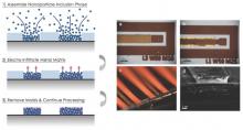
The micro-robot platforms (magnetic bases and end effectors) will be mass manufactured using a combination of precision manufacturing and microfabrication techniques. Rather than assembling discrete magnets into specific pole patterns, selective magnetization techniques will be used to “imprint” the desired pole pattern into mechanically contiguous layers. These methods will eliminate the need for assembly, and also facilitate the massive batch manufacture of many magnetic bases in parallel. Concurrently, end effectors will be microfabricated using suitable microfabrication technologies. The bases and end effectors will be combined together via monolithic co-fabrication or via wafer-scale batch-assembly processes.  

Large-area Manufacturing of Integrated Devices with Nanocomposite Magnetic Cores

As predicted by Moore's "law", the past few decades have seen massive reductions in the size of integrated circuits, enabling the portable, handheld devices now in everyday use. However, the components that power these devices have not experienced a similar size reduction. For example, the power adapter of a laptop computer is only modestly smaller than that two decades ago, and the printed circuit board inside a smart phone must dedicate between 20% and 40% of the board area for power conversion and management. To date, efforts towards miniaturization have been limited by both materials and manufacturing challenges. To address this gap, this research will study nanomanufacturing processes to facilitate the scalable synthesis of high quality magnetic nanoparticles and nanocomposite core materials and the fabrication of compact power inductors and transformers through assembly of these nanomaterials in a manner that is compatible with current manufacturing processes, such as silicon wafer or printed circuit board fabrication. This compatibility will enable fully integrated and compact system-on-chip or system-in-package power solutions. This research will be accomplished by fostering collaboration among disciplines including materials science, chemical engineering and electrical engineering. It will foster diversity in the profession by involving high school and undergraduate students in research activities and by broadening participation through the inclusion and engagement of women and underrepresented groups.

High Temperature Optical Sapphire Pressure Sensors for Harsh Environments

The primary objective of this research is to develop a high-bandwidth pressure sensor to provide benchmark, time-resolved, dynamic pressure data in high-temperature combustion environments. Specifically, these sensors will be designed to be embedded within a system and provide remote interrogation which will enable pressure to be measured in situ and on line under extreme conditions. Ultimately, this sensing technology will lead to better understanding and increased efficiency of complex power generation systems. In order to achieve this objective, research in sapphire laser micromachining and thermocompression bonding via spark plasma sintering technology will be conducted to enable fabrication of a fiber optic lever pressure sensor that uses a sapphire optical fiber for transduction of the pressure-induced diaphragm deflection. The proposed project will result in instrumentation-grade, high-temperature sensors that enable flush mounted measurements without sensor cooling. Furthermore, the use of optical techniques enables “passive” device operation, with electronics located remotely from the sensor. After fabrication and packaging, the pressure sensor will be rigorously characterized in acoustic plane wave tubes under both ambient and high-temperature conditions to determine its performance as a quantitative measurement device.

A Flush-Mount Piezoelectric MEMS Microphone for Aeroacoustic Flight Testing Applications

In their effort to locate, understand and mitigate the impact of noise sources on an aircraft, aeroacousticiansare in need of a high performance, low cost microphone to combat the increasing noise restrictions on commercial aircraft. Existing commercial sensors, even with their relatively high cost, in some cases constrain the quality and type of measurement that may be achieved. One such constraint is that the physical size and characteristics of the sensors limit the optimal locations in which the sensors may be placed. Previous generations of MEMS aeroacoustic microphones have failed to address the need for a sensor that can be packaged and installed with a smooth front surface to be used for boundary layer measurements in a fuselage array at cruise conditions. Additionally, these microphones must meet demanding requirements, including the sensing of high sound pressure levels (>160 dB) with low distortion (<3%) and high sensitivity stability (with respect to moisture and freezing) over temperatures from -60°F to 150°F. This work addresses the limitations of existing MEMS piezoelectric microphones used in aeroacoustic applications by incorporating through-silicon vias(TSVs) into the fabrication to eliminate the use of wirebondsthat affect the flow field and create an overall flush-mount microphone package.

A MEMS-based Fast-response Five-hole Probe with Optical Pressure Transducers

The goal of this research is to develop a MEMS-based Five-hole Probe(5HP) that is able to measure the localized velocity vector (both the velocity magnitude and direction) and the static and dynamic pressure, in steady and/or unsteady flow fields. Five optical pressure sensors located on the hemisphere tip of the 5HP provide all information that is needed to resolve the flow. This 5HP is expected to be able to provide high spatial resolution, high frequency response and is compatible with elevated temperature environments. A primary focus of this research is on the microfabrication and micromachining of a die that incorporates five optical transducers and its successive packaging process. The completed sensors will be tested in flow cells and wind tunnels at UF for the final calibration.

Directed Nanoparticle Assembly by Electrophoretic Deposition

This industry-sponsored project is funded by the MIST Center. The specific details of this project are confidential.


The Multi-functional Integrated System Technology (MIST) Center is an NSF Industry/University Cooperative Research Center (I/UCRC) led by the University of Florida and the University of Central Florida. Our mission is to facilitate integration of novel materials, processes, devices, and circuits into multi-functional systems through research partnerships between university, industry, and government stakeholders. With ~30 faculty participants from 6 different departments, the MIST Center serves as an early-stage research sandbox for developing next-generation smart systems in the Internet of Things era.

High-Performance CoPt Micromagnets

This industry-sponsored project is funded by the MIST Center.  The specific details of this project are confidential.


The Multi-functional Integrated System Technology (MIST) Center is an NSF Industry/University Cooperative Research Center (I/UCRC) led by the University of Florida and the University of Central Florida. Our mission is to facilitate integration of novel materials, processes, devices, and circuits into multi-functional systems through research partnerships between university, industry, and government stakeholders. With ~30 faculty participants from 6 different departments, the MIST Center serves as an early-stage research sandbox for developing next-generation smart systems in the Internet of Things era.

Processes for Manufacturing High-Performance Magnetic Materials in Electronic Systems

The objective of this research is to develop new manufacturing processes for the magnetic components used in modern electronic systems. The goal is improve the manufacturability, performance, and energy efficiency of power supplies and communication devices, while simultaneously reducing their size and weight. A novel process is used to combine the properties of two different magnetic materials by embedding magnetic particles of one type of material inside of a second material. The result is a new, hybrid magnetic material that exhibits improved material properties compared to existing materials. In the long run, these new magnetic materials are aimed to enable next-generation mobile electronics, communication systems, robotics, and medical devices. The project will strengthen an industry/university research partnership between the University of Florida and Electron Energy Corporation via technical exchange and a graduate student summer internship. The project also aims to broaden participation and retention of female and minority students in STEM career fields.

Ultrashort Pulsed Laser Micromachining of Sapphire Sensors for High Temperature Environments


As engineers seek to design more efficient gas turbines, they require a detailed understanding of fundamental thermal-fluid phenomena, as well as active control methods, in high-temperature environments. The high-temperature requirement is based on the increasing turbine inlet temperatures, which have risen to 1500 C, in combined cycle systems in order to improve turbine peak power and efficiency. The limited survivability of silicon-based MEMS sensors in high-temperature and harsh environments has caused researchers to investigate other materials for high-temperature MEMS-based sensors; more specifically sapphire.


Sapphire’s material properties make its entry into the world of high temperature sensors promising, but it also renders most traditional MEMS manufacturing methods impractical. Sapphire’s chemical inertness does not allow for effective dry or wet etching; consequently, a more effective method of machining the material is necessary. One potential solution is to use laser ablation, or material removal by vaporization due to localized heat input, to pattern the material. Femtosecond and picosecond pulsed lasers have shown the ability to reduce or eliminate the thermal damage issues of longer pulsed lasers. These lasers are classified as ultrashort pulse width because the duration of the pulse is so short that it does not allow for thermal conduction into the crystal lattice of the material.